The Project
Reimagining IoT for a Sustainable Future
GAIA is an ambitious EIC Pathfinder project pioneering a completely new paradigm for the Internet of Things: biodegradable, battery-less, and seamlessly integrated microelectronic systems that communicate using ambient cellular infrastructure.
Our long-term vision is a world where digital services blend into materials and objects naturally — without batteries, without electronic waste, and without the need for proprietary networks..
A New Class of Sustainable Microelectronics
GAIA builds on breakthroughs in biodegradable materials, transient electronics, antenna-based sensing, and ambient backscatter communication to create the first generation of fully transient IoT devices. These devices operate with ultra-low power, extract energy from surrounding RF signals, and naturally degrade at the end of their life cycle.
By embedding intelligence directly into everyday objects — from packaging to logistics and healthcare products — GAIA envisions a circular, infrastructure-aligned, and maintenance-free IoT ecosystem.
Co-Design Across Materials, Electronics & Networks
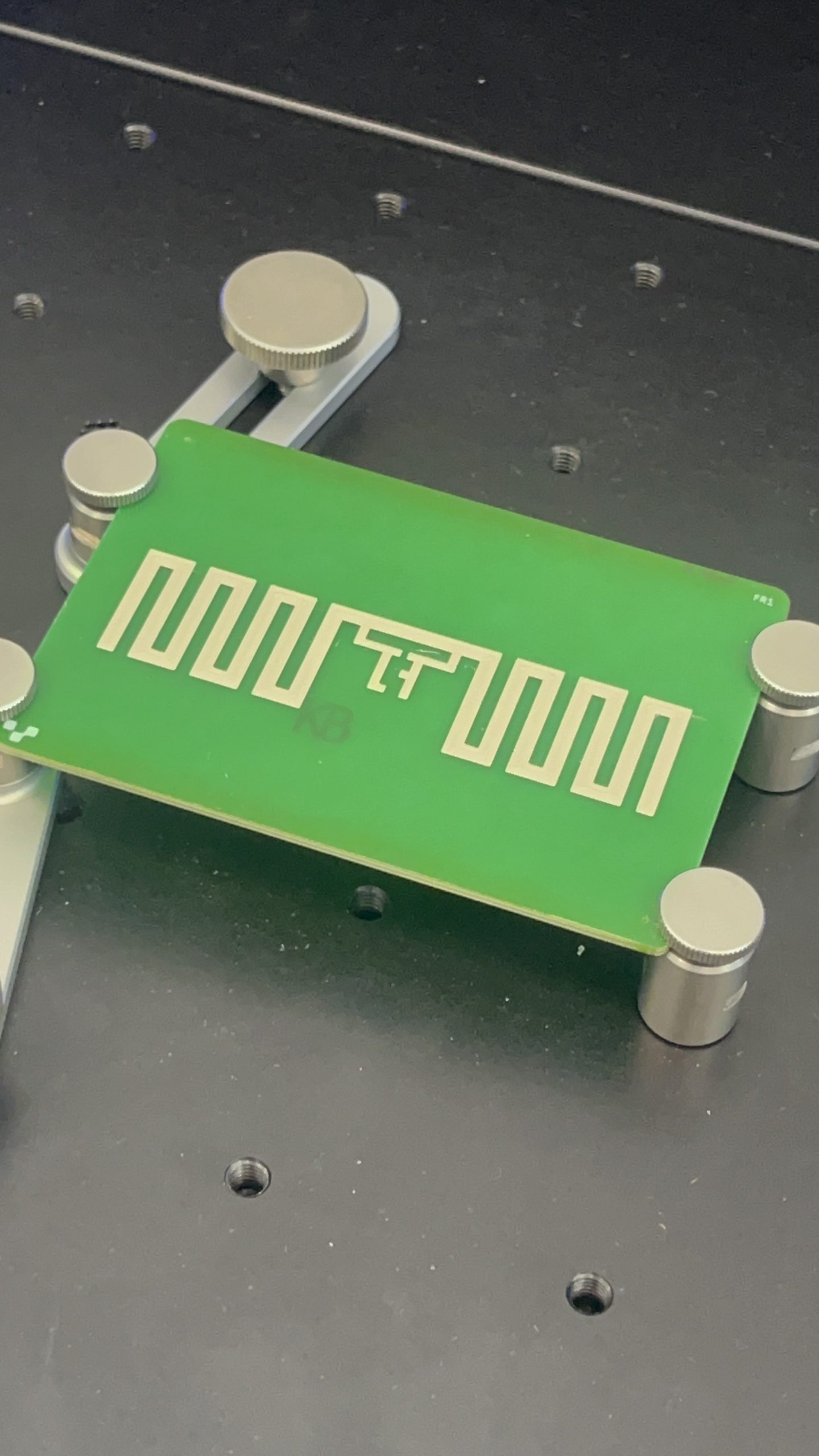
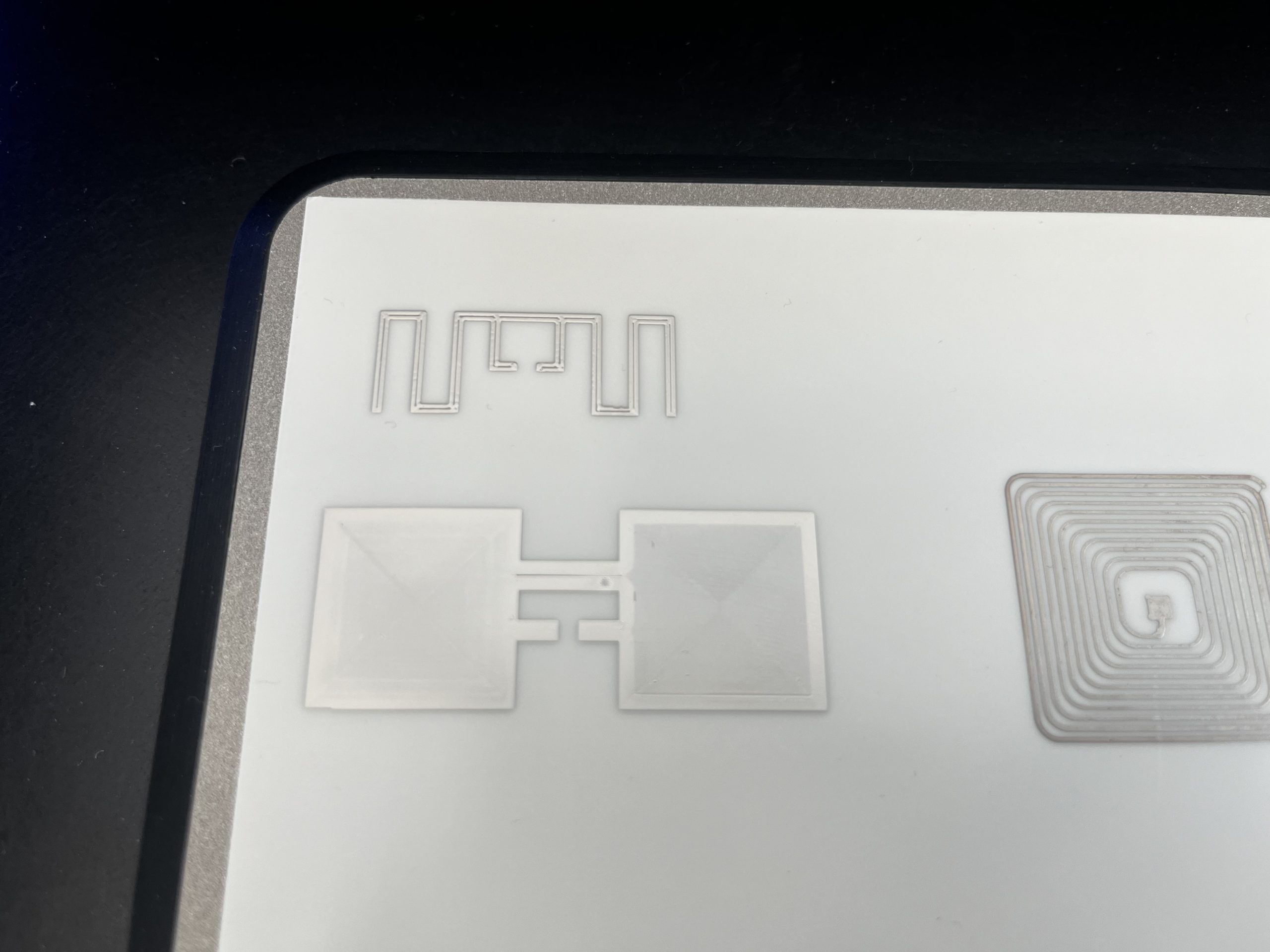
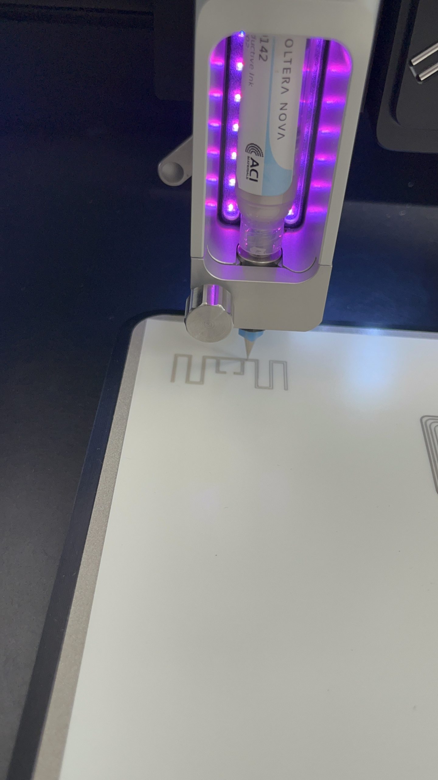
GAIA follows a holistic co-design approach spanning materials, circuits, antennas, and cellular networking:
- Advanced bio-based substrates optimized for RF performance
- Transient system-on-chip architectures integrating sensing, processing, and wireless backscatter
- Printed antennas engineered for efficiency on organic surfaces
- 5G/6G-compatible illumination protocols enabling large-scale device operation
- Edge-computing pipelines for robust inference from minimalistic sensing signals
This co-design approach ensures that conventional methodological and disciplinary boundaries are effectively overcome.
"GAIA’s breakthroughs support the EU Green Deal, the Digital Product Passport framework, and the transition toward zero-impact ICT systems."
Xavi Vilajosana
Innovation Potential
Innovative Technology
-
Biodegradable & Transient Electronics
GAIA develops microelectronic systems made from bio-based materials such as chitosan, cellulose, and transient metals. These components — processors, sensors, antennas and interconnects — are designed to function for a limited time and then safely decompose, eliminating e-waste. -
Ambient Backscatter Communication
Instead of generating their own radio signals, GAIA devices reflect and modulate existing cellular transmissions. This enables battery-free communication at extremely low power, compatible with emerging 5G/6G infrastructures. -
Wake-on-Sensor Intelligence
Novel material-based triggering mechanisms allow GAIA devices to remain dormant indefinitely and activate only when needed — for example, upon detecting a temperature threshold in a cold-chain package. -
Edge-Assisted Computing
Minimal local processing is combined with edge/cloud intelligence, enabling sustainable AI services even with ultra-simple hardware. This hybrid approach redefines how we design and distribute intelligence across IoT systems.
The Partners
University Oberta de Catalunya (UOC) – Spain
Role: Project Coordinator • Lead in Backscatter Communication, Cellular Protocols & Edge Architecture
UOC pioneers ultra-low-power wireless systems, cellular backscatter, and antenna-based sensing. As coordinator, UOC leads the GAIA architecture, illumination protocols for 5G/6G ambient IoT, and integration with edge/cloud systems. Its research shapes the project’s network-centric approach and overall vision for sustainable IoT.
FCT NOVA (NOVA) – Portugal
Role: Lead in Biodegradable Materials & Transient ElectronicsNOVA develops the biodegradable substrates, interconnects, and semiconductor materials at the core of GAIA’s transient electronic systems. Their expertise spans 2D materials, MXenes, ZTO-based devices, printed electronics, and fabrication techniques that enable transient VLSI and biodegradable memristive architectures.
Institut National de Recherche en Informatique et en Automatique (INRIA) – France
Role: Lead in Transient SoC Design & Integration
INRIA drives the development of GAIA’s transient system-on-chip, integrating sensing, processing, and cellular backscatter interfaces. Building on their SCuM and ultra-low-power RISC-V architectures, INRIA leads SoC design, modeling, co-simulation, and interfacing with biodegradable reservoirs and antennas.
Technische Universität Braunschweig (TUBS) – Germany
Role: Lead in Printed Electronics, Sensing & Wake-On Activation
TUBS specializes in hybrid microelectronics, sensor-triggered activation, and printed biodegradable interconnects. Their work enables GAIA’s wake-on-sensor mechanisms, ultra-low-power triggering, and robust integration between CMOS/transient electronics and biomaterial-based substrates.
Tampere University (TAU) – Finland
Role: Lead in Antenna Design, Printed RF Components & Biodegradable Sensing
TAU develops GAIA’s printed antennas, carbon-based conductive inks, and RF-ready biodegradable substrates. Their expertise in flexible and organic RF components ensures efficient backscatter communication and antenna-based sensing despite the constraints of transient materials.
Centre Tecnològic de Telecomunicacions de Catalunya (CTTC) – Spain
Role: Lead in 5G/6G Integration, Illumination Protocols & Edge-AI
CTTC brings deep expertise in 5G/6G radio systems, O-RAN networks, and edge compute architectures. They lead validation within real cellular infrastructure, design backscatter-compatible illumination strategies, and develop MEC-based inference pipelines that enable GAIA’s distributed AI-enabled sensing.
The Outcomes
2026
- TODO
- TODO
GAIA is a research consortium funded by the European Innovation Council (EIC) Pathfinder under Horizon Europe. Grant number: XXXXXXXX